

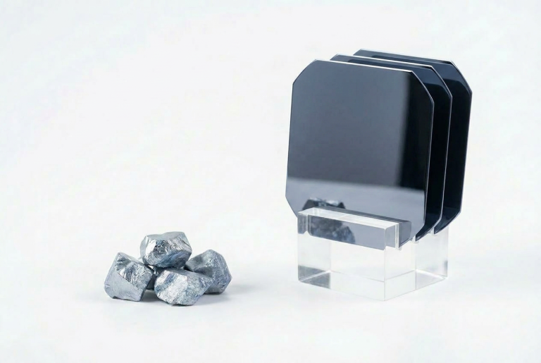
In the previous article, we read how a silicon ingot is cut into thin slices to form a wafer. At this stage, a wafer is a thin, ultra-pure piece of silicon — but it does nothing yet. If you shine sunlight on it, nothing happens. Before a wafer can generate electricity, it must first be converted into a solar cell. The most important step in this process is doping.
Why does pure silicon not conduct electricity?
Silicon is, by its very nature, a poor conductor. The atoms are arranged so neatly that there are hardly any free electrons. And free electrons are exactly what you need for an electric current — an electric current is nothing more than moving electrons.
By adding small amounts of another element to the silicon, you can change that. This is called doping. The amounts involved are extremely small — sometimes just one foreign atom per billion silicon atoms — but the effect on conductivity is significant.
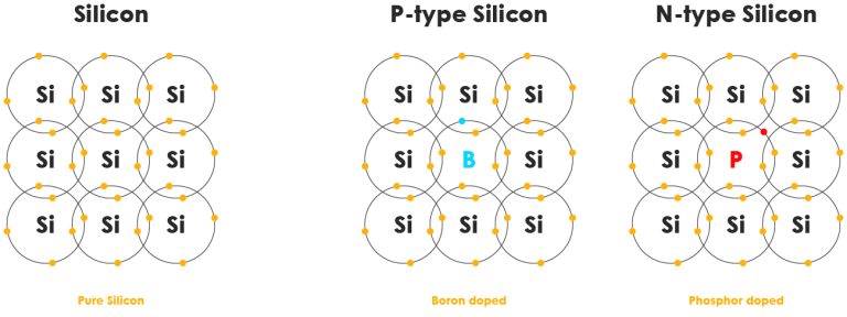
Two types of doping: n-type and p-type
Two different layers are created, each with a different dopant.
The first layer is n-type silicon. Phosphorus is added to achieve this. Phosphorus has one more electron than silicon in its outermost shell. That extra electron does not fit into the crystal structure and is free to move. The result is a layer of silicon with an excess of free electrons.
The second layer is p-type silicon. Boron is used for this. Boron has exactly one electron fewer than silicon. This creates ‘holes’ in the structure — places where an electron could be, but isn’t. These holes behave as positive charges and can also move through the material.
The p-n junction: the heart of the solar cell
When the n-type and p-type layers are placed against each other, a special region is formed at the boundary between the two layers: the p-n junction. At this boundary, electrons move from the n-side towards the holes on the p-side until equilibrium is reached. In the process, an electric field builds up.
That electric field is what powers the solar cell.
How does the solar cell generate electricity?
Sunlight consists of photons — tiny packets of energy. When a photon strikes the solar cell, it transfers its energy to an electron in the silicon. That electron is released and begins to move.
The electric field at the p-n junction directs that electron in one direction. Via metal contacts on the front and back of the cell, the electron flows through an external circuit — through your devices — and then returns. That is the current generated by your solar panel.
Further processing of the wafer
After the doping process, the wafer undergoes a number of further treatments before it becomes a fully-fledged solar cell.
First, the cell is coated with an anti-reflective layer. Bare silicon reflects a lot of light, which reduces efficiency. A thin layer of silicon nitride prevents this. This layer also gives solar cells their characteristic dark blue or black colour.
Next, the metal contacts are applied. On the front, these are thin silver lines — as thin as possible, because any line that blocks light represents wasted energy. On the back, there is a wider layer of metal that conducts the current.
Finally, the cell is passivated. The edges and surface are chemically treated to prevent electrons from escaping in the wrong places. This increases the cell’s efficiency.
From wafer to solar cell
Once all these steps have been completed, the wafer becomes a functioning solar cell. A single cell generates approximately 0.5 volts. Several cells are connected in series to produce a usable amount of electricity — the number of cells required depends on the size and type of the end product.
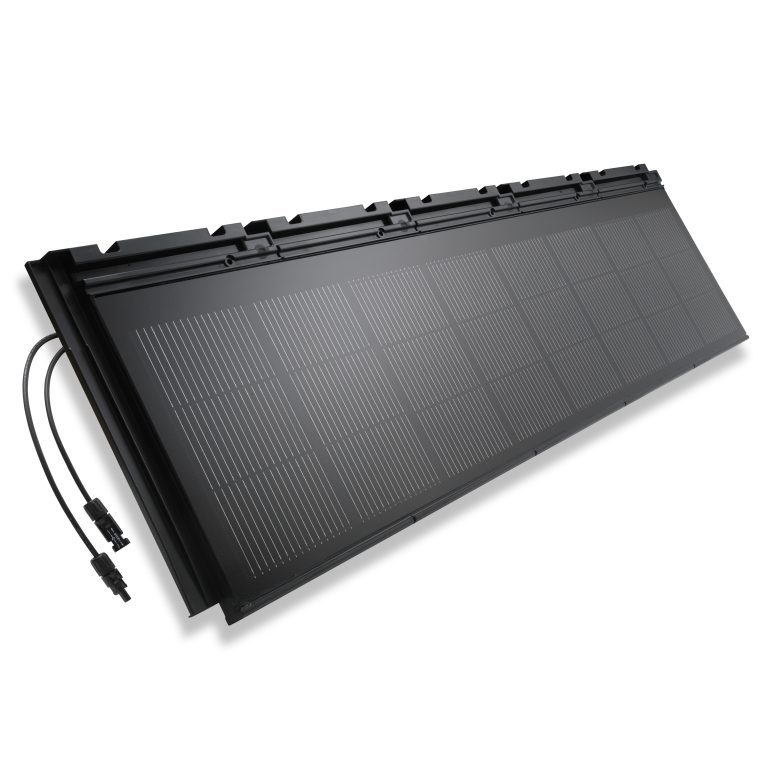
At Solinso, we incorporate these solar cells into our solar roof tiles. They are more compact than a traditional solar panel, but are based on the same technology — from a grain of sand to a fully functional solar cell.