

In the previous article, we saw how raw quartz is converted, step by step, into polysilicon — small, shiny grains of almost pure silicon. But a bag of grains does not make a solar panel. Before it can be turned into a solar cell, the silicon is first converted into an ingot: a large cylinder of crystalline silicon with a very specific structure. In this article, we explain how such an ingot is made, and why that crystal structure is so important.
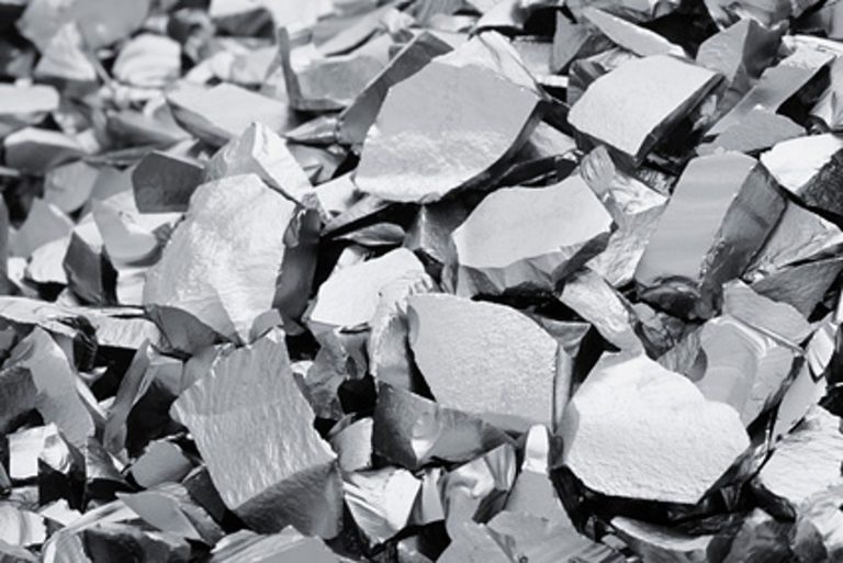
From granules to liquid silicon
The process begins with melting the polysilicon. The granules are placed in a large crucible made of quartz glass or graphite and heated to around 1420 degrees Celsius — the melting point of silicon. That sounds hot, and it certainly is: by way of comparison, lava from a volcano is around 1200 degrees.
During the heating process, the temperature is closely monitored. If it is too hot, the quality of the silicon suffers; if it is too cool, it solidifies too quickly. Once all the grains have completely melted, a bath of liquid, ultra-pure silicon is formed. That liquid silicon is the starting point for the next step: growing an ingot using the Czochralski process.
How is an ingot grown?
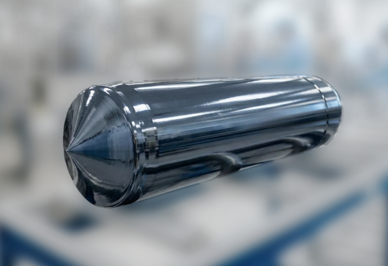
An ingot is a large, cylindrical rod of crystalline silicon. It is not cast or pressed, but is slowly grown from molten silicon. This is done using the Czochralski process, named after the Polish scientist Jan Czochralski, who discovered it in 1916.
The Czochralski process works as follows. A small piece of solid silicon, known as a seed crystal, is immersed in the molten bath. This seed crystal already has the correct crystal structure. The molten silicon adheres to it and begins to crystallise in the same structure.
As the seed crystal is slowly pulled upwards whilst rotating, an ever-larger cylinder forms at the bottom. The speed at which this occurs, and the temperature of the bath, determine the quality and diameter of the ingot.
The end result is an ingot approximately one metre long and up to 30 centimetres in diameter. Such an ingot can easily weigh between 100 and 300 kilograms.
Why is the crystal structure so important?
Inside the ingot, all the silicon atoms are arranged in a perfectly repeating pattern. This is known as a monocrystalline structure. This structure is important because electrons can move through it easily — and that is exactly what you need to generate electricity efficiently.
There is also a cheaper alternative: polycrystalline silicon. In this process, the silicon is cast into a block rather than grown slowly. The atoms are then not arranged in a single continuous pattern, but in a mixture of several small crystal orientations. This makes production cheaper, but efficiency slightly lower. Older solar panels with a blue speckled pattern are often made of polycrystalline silicon.
From ingot to wafer
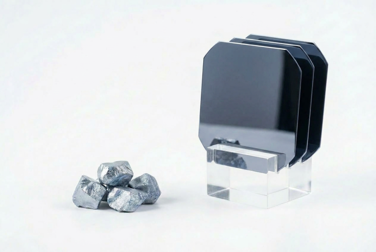
Before the ingot can be processed further, its sides are ground straight. The cylindrical shape is useful during growth, but for sawing you want a more rectangular shape.
The ingot is then cut into thin slices: wafers. This is done using a wire saw — a system comprising thousands of thin wires that cut through the silicon simultaneously. In a single cutting operation, hundreds of wafers are cut at once.
A wafer is approximately 170 micrometres thick. That is thinner than two human hairs placed side by side. They are fragile and, after being cut, are carefully cleaned and checked for damage.
However, some material is always lost as sawdust during the cutting process. This is wasted pure silicon, and manufacturers do their best to reuse it as much as possible.
Ready for the next step
What remains are hundreds of thin, shiny silicon wafers. At this stage, they do not yet interact with light — that changes in the next step. The wafers are treated so that they can actually generate electricity as soon as sunlight hits them. You can read about how this works in the following article on cell doping.